

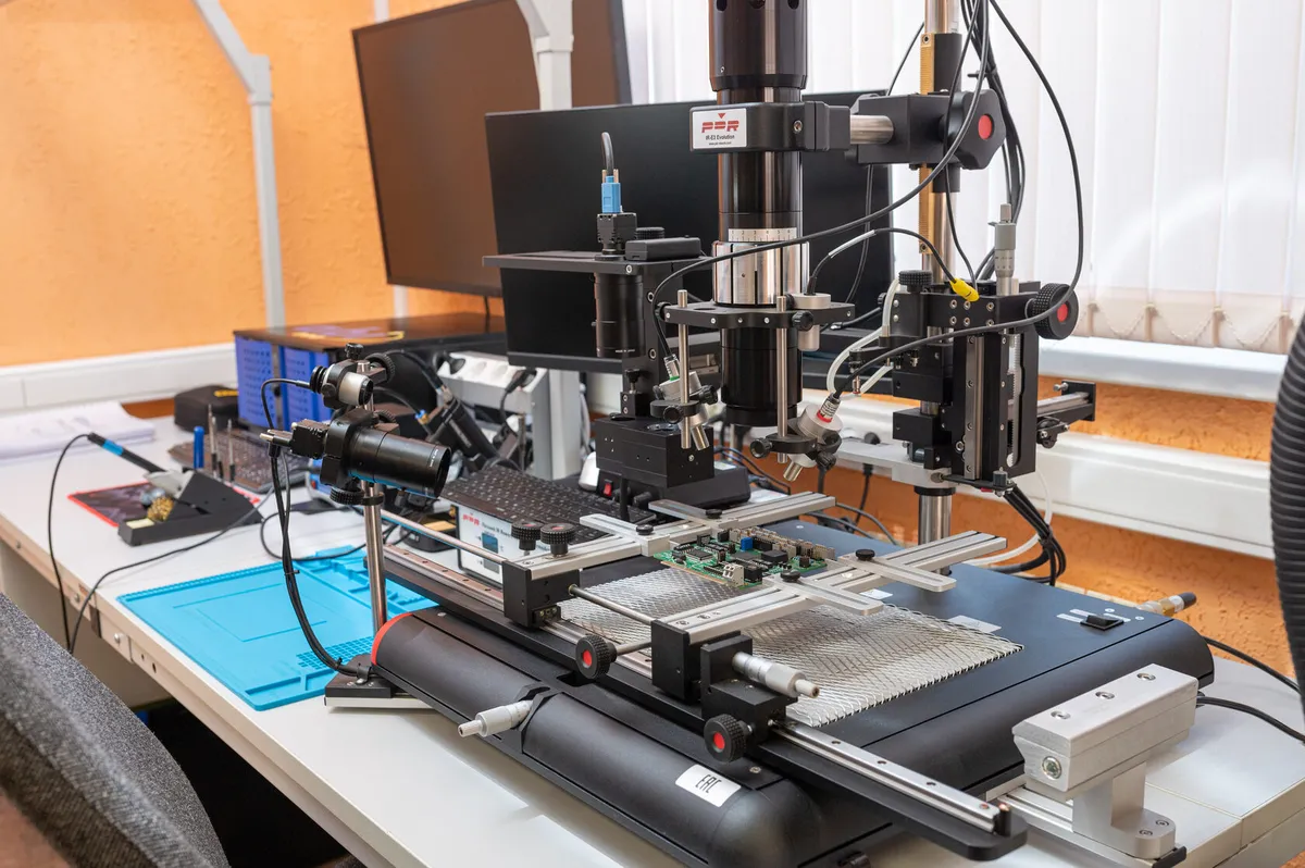
Localizing a fault down to a single component on BoardMaster is the foundation of predictable industrial electronics repair. Instead of blindly swapping whole assemblies, we pinpoint the exact point of failure on the board and restore only what actually broke. Below we explain how the diagnostic process on ABI BoardMaster works, why it reduces repair cost, and when we combine it with thermal imaging and X-ray.
What VI testing on ABI BoardMaster is
BoardMaster from ABI Electronics is an analog signature analysis system, better known as VI testing (Voltage-Current characteristic). The principle is simple: a current-limited AC signal is applied to a component pin, and the instrument plots current against voltage. Every electronic component has its own characteristic signature. A resistor produces a sloped line, a capacitor an ellipse, and a healthy p-n junction a distinctive knee.
The key advantage of the method is that testing runs without applying operating power to the board. That means we can safely probe nodes that would short out on power-up or drag adjacent circuits down with them. On industrial boards, where a single power switch can damage half the schematic, this matters a great deal.
Analog signature and known-good comparison
A component signature on its own says little until there is something to compare it against. So the core working method is known-good comparison. We capture the VI characteristics from a proven reference board, then run the same points on the faulty sample. The instrument highlights deviations circuit by circuit and shows immediately where the signature has drifted from normal.
The nature of the deviation reveals the type of defect. A capacitor ellipse shifted downward points to leakage or breakdown. A straight line instead of a junction knee signals a shorted semiconductor. A broken characteristic means an open circuit or a cold solder joint. This approach sharply narrows the search area: instead of the whole board, we work with a few suspect points.
When no reference board is available, we use signature libraries and compare identical channels within the same board against each other. Many industrial modules contain repeated sections, and a working channel becomes the reference for the failed one.
It is worth saying a word about test modes. The VI characteristic is captured across different ranges of voltage, current and signal frequency. A low voltage gently checks sensitive inputs, a higher one better reveals breakdowns in power circuits, and changing the frequency helps tell a capacitor from an inductor. The engineer selects the range to suit the type of circuit, so the same pin can be assessed from several angles, and a defect visible only in a particular mode is not missed.
Step by step localization
Diagnostics on BoardMaster follow a repeatable route so the result does not depend on the engineer’s mood.
- Visual inspection and signature capture on the power rails. We check power circuits for shorts and leakage first, since these most often pull a board into failure.
- Running connectors and edge contacts through the known-good comparison. We look for broken traces, contact degradation and cracks after vibration.
- Step by step signature comparison of active components: ICs, switches, regulators. Deviations are recorded in the report.
- Verifying the identified point under load and confirming the diagnosis before replacing the component.
The output is not a guess but a documented set of deviations tied to specific positions on the board. This is exactly what lets us agree on timelines and cost before any soldering begins.
Where VI testing is complemented by other methods
VI testing is powerful, but it is not the only tool. Some defects appear only when the board is running or stay hidden under a component body, and here we bring in adjacent methods.
Thermal imaging catches parts that heat up beyond normal under load. Leakage that the signature shows as a slight deviation looks like a clear hotspot on a heat map. We covered this in detail in our article on thermal scanning a board before repair.
X-ray inspection is needed where pins are physically inaccessible to a probe. Under BGA components the solder is invisible to the eye, and joint quality can only be assessed by X-ray. There is a separate breakdown in our article on BGA solder joint inspection.
The combination of three methods gives a full picture: BoardMaster shows the electrical behavior of circuits, thermal imaging the thermal behavior, and X-ray the physical state of hidden joints.
ESD and workbench discipline
Precise diagnostics are pointless if we introduce new defects along the way. Industrial electronics are sensitive to electrostatic discharge, so all work follows ESD requirements: grounded wrist straps, antistatic mats, humidity control and conductive containers for boards.
We carry out repair operations to IPC-7711 and IPC-7721 standards, which describe the accepted methods for rework and repair of printed boards and solder joints. This guarantees that after repair the board meets the same quality requirements it had at manufacturing. A strict process is part of our philosophy of repair, not waste.
What the customer gets
For the customer, precise fault localization turns into concrete benefits. A transparent report before work starts shows exactly what failed, so approving timelines and cost happens without surprises. Component-level repair instead of replacing the whole module noticeably reduces cost, especially for obsolete or discontinued boards that can no longer be purchased.
We apply this approach in projects for rail transport, metro systems and marine electronics, where equipment downtime costs more than the repair itself.
If you have a board that the supplier only offers to replace as a whole, bring it in for diagnostics. We will capture the signatures, localize the failure and tell you honestly what can be restored and what cannot. You can discuss the task through our contact page.