

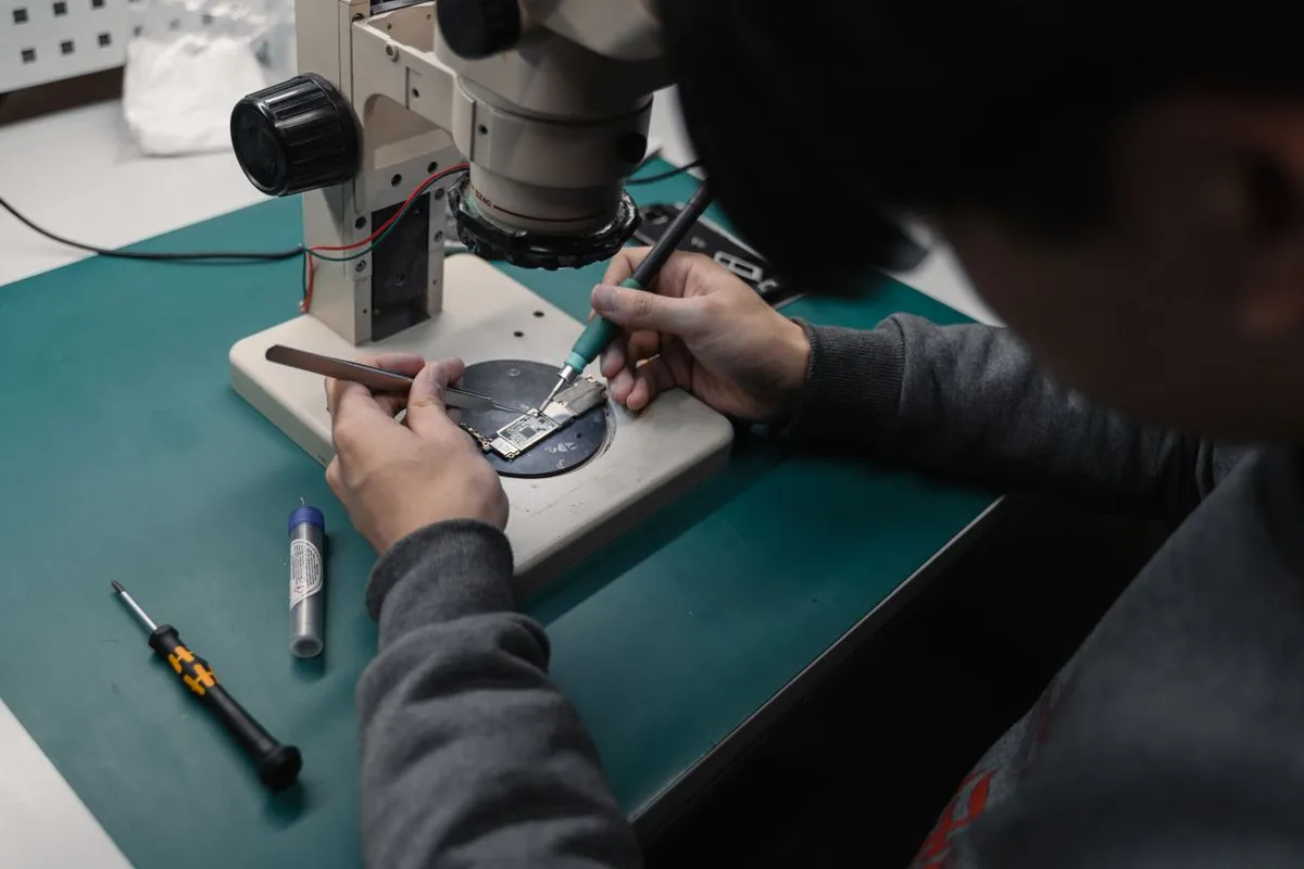
A stereo microscope for soldering and micro-rework is one of the key instruments in our workshop, and without it quality component-level repair of modern electronics is simply impossible. Assembly density has grown so much that many defects are invisible to the naked eye: a micro-crack in a joint, a lifted lead, a hair of solder bridging two adjacent pads. Under magnification all of this becomes obvious. Below we explain in detail what exactly we do under the microscope and why a reliable result cannot be guaranteed without it.
Why a stereo microscope is needed for repair
An ordinary magnifier gives a flat image and does not let you judge the volume of a solder joint. A stereo microscope provides two independent optical channels, that is a true three-dimensional image with a sense of depth. This is essential for soldering: the iron tip, the tweezers and the component lead all sit at different heights, and without the stereo effect you cannot precisely land the tip on a pad that measures fractions of a millimetre.
We work across a range of magnification, from a low overview to high detail. Low magnification is convenient for inspecting the whole board and locating the problem area, while high magnification is used to control a specific joint. A long working-distance objective leaves enough room between the lens and the board to fit both an iron and a hot-air nozzle underneath. Ring LED lighting removes shadows and glare, which is critical when you need to tell a shiny sound joint from a dull cold one.
Inspecting solder joints
The first thing the microscope is used for is visual inspection of solder joints. Under magnification we assess the shape of the solder fillet, the wetting of the pad and the lead, and the presence of voids or foreign inclusions. A good joint has a concave, shiny fillet that evenly wraps around the lead and the pad. Any deviation from this shape is a signal to look more closely.
What we look for during inspection:
- Insufficient or excessive solder on the joint.
- Non-wetting and partial wetting, where the solder has not flowed across the pad.
- Solder balls and bridges between adjacent leads.
- Flux residue, which produces leakage currents under load.
- Mechanical damage to pads and lifted traces.
We carry out this inspection both on the incoming board, to understand the assembly history, and after every intervention of our own, to confirm the quality of the work.
Finding micro-cracks and cold joints
The most treacherous defects are micro-cracks and cold joints. They are not visible at a glance, yet they are exactly what causes floating faults: the device works, then freezes on warm-up or after vibration. Under the microscope a crack in the fillet looks like a thin dark line along the edge of the solder, while a cold joint appears as a dull, grainy, almost swollen connection without proper wetting.
Cracks appear especially often around heavy and thermally loaded components: connectors, power parts, large electrolytic capacitors. Equipment arriving from rolling stock and vessels carries constant vibration load, and cracks along connector leads are a typical finding on such boards. The microscope lets us localise this defect precisely, rather than reflowing the whole board blindly.
We complement visual inspection with a light mechanical test: under magnification we gently load the suspect node with a probe and watch for any movement. A lead that moves under load is an almost certain sign of a hidden crack in the joint.
Working with 0201 and 0402 components
Passive components in the 0201 and 0402 sizes are resistors and capacitors the size of a grain, literally fractions of a millimetre. By hand, without optics, you can neither place them straight nor remove them without disturbing their neighbours. Under the microscope this work becomes controllable.
When replacing small parts, under magnification we remove the old component with hot air or an iron, clean and tin the pads, precisely position the new part with tweezers and solder both terminations. The microscope immediately shows whether the component is centred on the pads, whether there is a tombstoning effect where the part lifts on one end, and whether there is a bridge to a neighbouring part. All of this is corrected on the spot, at the same magnification.
QFN leads and the BGA edge row
QFN and QFP packages with a lead pitch of a few tenths of a millimetre require constant control under the microscope. We check every lead for wetting and look for non-wets and bridges, which form especially easily between the legs. The thermal pad under a QFN is also monitored: at the edge you can see solder escaping from under the body, which indirectly confirms the quality of the central-pad joint.
With BGA packages we work under the microscope around the perimeter. The balls themselves are hidden under the body and are only visible on X-ray, but the outer row lets us judge the height and shape of the edge balls, the evenness of the component seating and the absence of shift. We obtain the full picture of the hidden joints separately, as described in detail in our article on BGA joint inspection. Here the microscope and the X-ray complement each other: one gives edge control and precise hand work, the other reveals what is under the body.
Quality control to IPC-A-610
We do not judge soldering by eye in a like-it-or-not fashion. Visual inspection under the microscope follows the criteria of the IPC-A-610 standard, which describes the acceptability of electronic assemblies: fillet shape, minimum acceptable wetting, allowable void sizes, board cleanliness requirements and the absence of bridges. The standard sets an objective bar, and our joints after repair must meet it.
The removal, soldering and rework operations themselves we perform to the IPC-7711 and IPC-7721 methods, the standards for repair and rework of printed assemblies. All work is done in accordance with ESD requirements, that is protection against static electricity: a grounded wrist strap, an antistatic mat and tools. Under the microscope it is easy to see when a previous repair was done without observing these rules, and such boards often have to be redone from scratch.
Precise hand soldering under magnification
Beyond inspection, the microscope is also a workstation for the soldering itself. Many operations are physically impossible without magnification: restoring a lifted pad, soldering a thin jumper wire when repairing a trace, replacing a lead on a fine-pitch connector, removing conformal coating pointwise over the exact spot.
Working under the microscope also changes the technique itself: movements become finer and more precise, the iron lands squarely on the pad, and the solder dose is metered visually. We see the moment of wetting and lift the tip at exactly the right time, without overheating the joint. This is how repeatable quality is achieved, rather than a random result.
After soldering, the node is always cleaned of flux, and if needed the conformal coating is restored. A final check under the microscope is the last step before the board goes to a load test, which we described in our article on post-repair burn-in.
What we do under the microscope
To bring it together, under the stereo microscope we: inspect solder joints on arrival and after repair, search for micro-cracks and cold joints, replace 0201 and 0402 components, control QFN leads and the BGA edge, restore pads and traces, perform precise hand soldering and check the result against IPC-A-610. This is not a separate service but a mandatory part of every component-level repair.
The microscope does not do the work for the technician, but it gives the ability to see what is hidden and to work with a precision unavailable by eye. That is why we never release a board without a final check under magnification.
If you have a board with dense surface-mount assembly, a suspected hidden crack in a joint, or a failed previous repair, bring it to us. We will inspect the joints under the microscope and tell you honestly what needs to be done. You can discuss your task through our contact page.